

Michael K L Man
Okinawa Institute of Science and Technology Graduate University, Japan
Title: Imaging electrons motion in semiconductor materials
Biography
Biography: Michael K L Man
Abstract
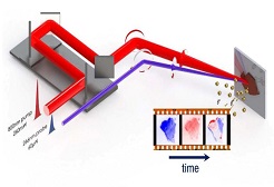
Unveiling the fundamental mechanisms in semiconductor devices helps to unlock new paths toward better device performance and design. One of the key processes behind all device structures, is the internal motion of electrons through semiconductor materials due to applied electric fields or excitation of photocarriers. The ability to image the motion of electrons would further our understanding in these charge transfer processes, but requires both high spatial and time resolution. In the study of electron dynamics in materials, ultrafast optical techniques provide excellent temporal resolution, but are limited to spatial resolution. On the other hand, electron microscopy techniques provide very good spatial resolution, but offer poor temporal resolution. Here, by combining femtosecond pump-probe techniques with photoemission electron microscopy, we can track the motion of electrons through space and time, and gain access to the evolution of these electrons in energy and momentum space. In our recent publication, we have imaged the flow of electrons from high to low energy states in a InSe/GaAs semiconductor heterostructure shortly after photoexcitation, which essentially visualized the fundamental operating phenomena of solar cell devices. At the instant of photoexcitation, our measurement revealed the highly non-equilibrium distribution of photoexcited carriers in energy and space. Thereafter, in response to the out-ofequilibrium photocarriers, we observed the spatial redistribution of charges, which results in the formation of an internal electric fields that impede and finally stop the flow of electrons. By stitching together images taken at different time-delays, we created a movie lasting a few trillionths of a second of the electron transfer process in the photoexcited semiconductor heterostructure. Quantitative analysis and theoretical modeling of spatial variations in the video provide insight into operation of solar cells, the physics of 2D van der Waals materials, and other optoelectronic devices in general.
Recent Publications
- M. K. L. Man, A. Margiolakis, S. Deckoff-Jones, T. Harada, E. Wong, M. B. M. Krishna, J. Madéo, A. Winchester, S. Lei, R. T. Vajtai, P.M. Ajayan and K.M. Dani, “Imaging the motion of electrons across semiconductor heterojunctions”, Nature Nanotechnology 183 (2016).
- S. Deckoff-Jones, J. Zhang, C. E. Petoukhoff, M. K. L. Man, S. Lei, R. Vajtai, P. M. Ajayan, D. Talbayev, J. Madéo and K. M. Dani, “Observing the interplay between surface and bulk optical nonlinearities in thin van der Waals crystals”, Scientific Reports 6, 22620 (2016).
- M. K. L. Man, S. Deckoff-Jones, A. Winchester, G. Shi, G. Gupta, A. D. Mohite, S. Kar, E. Kioupakis, S. Talapatra and K. M. Dani, “Protecting the properties of monolayer MoS2 on silicon based substrates with an atomically thin buffer”, Scientific Reports 6, 20890 (2016).
- B. M. K. Mariserla, M. K. L. Man, S. Vinod, C. Chin, T. Harada, J. Taha-Tijerina, C. S. Tiwary, P. Nguyen, P. Chang, T. N. Narayanan, A. Rubio, P. M Ajayan, S. Talapatra and K. M. Dani, “Engineering Photophenomena in Large, 3D Structures Composed of Self-Assembled van der Waals Heterostructure Flakes”, Advanced Optical Materials 3, 1551-1556 (2015).
- K.L. Man and M.S. Altman, “Small-angle lattice rotations in Graphene on Ru(0001)”, Phys. Rev. B 84, 235415 (2011).