Day 2 :
Keynote Forum
Elias Siores
University of Bolton, UK
Keynote: Hybrid photovoltaic-piezoelectric flexible device for energy harvesting from nature
Time : 08:00-08:25

Biography:
Elias Siores is the Provost and Director of Research and Innovation, Bolton University. He completed his BSc, MSc, MBA and PhD in UK and pursued his academic career in Australia (Sydney, Brisbane and Melbourne) and Asia (Hong Kong, Dong Guan) before returning to Europe (UK) as a Marie Curie Fellow. His R&D work concentrated on advancing the science and technology in the field of “Automated non-destructive testing and evaluation including ultrasound, acoustic emission and microwave thermography. His recent R&D work focuses on Smart/Functional Materials and Systems Development. In this area, he has developed electromagnetic, electrorheological, photovoltaic and piezoelectric smart materials based energy conversion systems for renewable energy, medical, health care and wearable devices. He has published over 300 publications including 8 patents. He has been a member of editorial boards of international journals and a Fellow of IOM, TWI, IEAust, SAE and WTIA. He has received 15 awards in his career for R&D achievements.
Abstract:
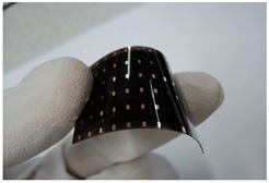
Statement of the Problem: Photovoltaic materials have unique conversion characteristic that they can convert sun light to electrical energy. However, photovoltaic energy can be expensive if the solar radiation in a particular region is not abundant. When the solar radiation is scarce in a region, there is presence of wind and rainfall. If flexible solar cells are coupled with flexible piezoelectric films then the hybrid structure can generate energy from solar radiation, wind and rainfall. This work focuses on nontransparent hybrid structure which contains copper and aluminum electrodes and eliminates the use of costly indium tin oxide (ITO).
Methodology & Theoretical Orientation: Hybrid film has been developed by depositing organic photovoltaic cell based on P3HT and PCBM on a piezoelectric film under ambient room conditions and tested. Findings: The hybrid film produced an open circuit voltage (Voc) of 0.45 V and a short circuit current density (Jsc) of 0.43 mA/cm2 under solar simulator and a peak power of 85 μW when subjected to a turbulent wind speed up to 10 m/sec (36 km/ hour) in a custom built wind tunnel.
Conclusion & Significance: HPP film has been developed by depositing organic photovoltaic cell based on P3HT: PCBM on a piezoelectric film under the ambient room conditions. HPP film produced was ITO free and cost effective since the usage of expensive clean room procedure has been eliminated. Experimental results proved that the HPP film produced was able to convert both wind energy and solar energy into electrical energy.
Recent Publications
- Vatansever D, Hadimani RL, Shah T, Siores E (2013) Hybrid Photovoltaic-Piezoelectric Flexible Device for Energy Harvesting from Nature. Advances in Science and Technology 77: 297-301
- Hadimani RL, Bayramol DV, Soin N, Shah T, Qian L, Shi S, Siores E (2013) Continuous production of piezoelectric PVDF fibre for e-textile applications. Smart Materials and Structures, 22(7): 075017.
- Hadimani MLR, Siores E, Vatansever D, Prekas K (2011) U.S. Patent Application No. 13/876,162.
- Soin N, Shah TH, Anand SC, Geng J, Pornwannachai W, Mandal P, Siores E (2014) Novel “3-D spacer” all fibre piezoelectric textiles for energy harvesting applications. Energy & Environmental Science, 7(5): 1670-1679.
- Matsouka D, Vassiliadis S, Prekas K, Bayramol DV, Soin N, Siores E (2016) On the Measurement of the Electrical Power Produced by Melt Spun Piezoelectric Textile Fibres. Journal of Electronic Materials, 45(10): 5112-5126.
Keynote Forum
Alex guskov
Institute of Solid State Physics of RAS, Russia
Keynote: The decomposition of the solution during the formation of eutectic composites
Time : 08:25-08:50

Biography:
Alex Guskov completed his PhD in 1982 at Physical Institute of Russian Academy of Sciences. He worked at Institute of Solid State Physics, Russian Academy of Sciences and investigated the influence of interaction of laser radiation and a solid. Simultaneously, he was engaged in application of technological processes in manufacture of electronic devices. Now his research interest focuses on “Heat mass transfer during the phase transition”.
Abstract:
Motivation Research: Explanation and prediction of the distribution of components in the crystallization solutions causes great difficulties. One reason for this is the assumption that during crystallization the solution is in the metastable state. The decomposition of the solution occurs by binodal scenario in this case.
Aim: The purpose of this study is to show that in many cases the solution during crystallization is in an unstable state. The unstable condition leads to decomposition of the solution by spinodal scenario.
Methodology & Theoretical Orientation: Experimental demonstration of spinodal decomposition of the solution is conducted by means of video shooting. Locally configuration thermodynamic model is used to explain the state changes of the solution during the phase transition. This model allowed adding additional coordinate - mixing energy in the equilibrium phase diagram. Boundary of the spinodal area of the solution is built into the new coordinates. Spinodal defines curve the dynamic equilibrium that must be considered in the calculations of the processes of interphase mass transfer.
Findings: The possibility of spinodal decomposition of the solution during its crystallization significantly alters the representation of interphase mass transfer. Many cases of the redistribution component during the phase transition cannot be explained without taking into account of spinodal decomposition.
Conclusion & Significance: Spinodal decomposition of the solution explains the process of formation of a periodic distribution of the eutectic composites. The layer of the unstable solution is localized in front of the unstable interface. The unstable solution decomposes into phases have a composition close to the eutectic composition of the solid phases. The period of alternation of these phases is set by the period of instability of the interface. Experiments show that the formation of dendrites in the two-phase zone and extremum of the component concentration close to interface also occurs in the spinodal decomposition scenario.
Recent Publications
- Guskov A.P. (2016) The decomposition of the solution during the formation of eutectic composites. COMPOSITES and NANOSTRUCTURES, Volume 8, N3, pp. 2-15. (in Russian)
- Alex Guskov, (2014) On Linear Analysis of the Movement of the Interface under Directed Crystallization. Advances in Chemical Engineering and Science, 4, 103-119.
- A. P. Guskov, L. P. Nekrasova, A. S. Gornakova, and I. A. Shikunova (2014) Crystallochemiluminescence of Solutions Crystallography Reports, Vol. 59, No. 5, pp. 758–761.
- A. Guskov, L. Nekrasova. (2013) Decomposition of Solutions in Front of the Interface Induced by Directional Crystallization. Journal of Crystallization Process and Technology. 3, 170 - 174.
- Guskov A.P., Nekrasova L.P., Ershov A.E., Kogtenkova O.A. (2013) The decomposition of the solution in the interface under directional solidification. Materilovedenie - Materials Science, No. 10, pp. 10-15 (in Russian).
- A.Guskov, (2012) Qualitative Analysis of Interface Behavior under First Order Phase Transition. Journal of Crystallization Process and Technology, 2, pp. 25-29.
- A. P. Guskov (2009) The period of decay of a nonequilibrium solution at the directed crystallization. Materials Science No 10, p. 9-13 (in Russian).
- A.Gus’kov, A.Orlov (2009) Influence of an interphase nonequilibrium solution layer on formation eutectic pattern. Materials Science No 12, p. 2-6 (in Russian).
Keynote Forum
Udo Schwingenschloegl
King Abdullah University of Science & Technology,Saudi Arabia
Keynote: Designing topological states by pressure, strain and functionalization
Time : 08:50-09:15

Biography:
Udo Schwingenschlogl is a Professor of Materials Science & Engineering at King Abdullah University of Science and Technology (KAUST), Saudi Arabia. He previously worked at International Center of Condensed Matter Physics in Brasilia, Brazil, and University of Augsburg, Germany. His research interests in condensed matter physics and first-principles materials modeling focus on “2D materials, interface and defect physics, correlated materials, thermoelectric materials, metal-ion batteries, nanoparticles and quantum transport”.
Abstract:
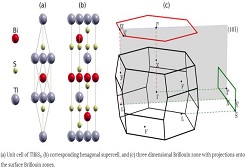
Various examples of the design of topological states by means of first-principles calculations are discussed. The presentation focusses on the design parameters: Pressure, strain and functionalization. TiTe2 is found to be unusually accessible to strain effects and the first compound that under hydrostatic pressure (up to experimentally reasonable 30 GPa) is subject to a series of four topological phase transitions, which are related to band inversions at different points of the Brillouin zone. Therefore, TiTe2 enables experimental access to all these transitions in a single compound. Phase transitions in TlBiS2 and TlSbS2 are identified by parity analysis and by calculating the surface states. Zero, one and four Dirac cones are found for the 111 surfaces of both TlBiS2 and TlSbS2 when the pressure grows, which confirms trivial-nontrivial-trivial phase transitions. The Dirac cones at the M points are anisotropic with large out-of-plane component. TlBiS2 shows normal, topological and topological crystalline insulator phases under hydrostatic pressure, thus being the first compound to exhibit a phase transition from a topological to a topological crystalline insulator. Monolayer arsenic and arsenic antimonide are semiconductors (direct band gap at the Γ point), fluorination results for both compounds in Dirac cones at the K points. Fluorinated monolayer arsenic shows a band gap of 0.16 eV due to spin-orbit coupling and fluorinated arsenic antimonide a larger band gap of 0.37 eV due to inversion symmetry breaking. Spin-orbit coupling induces spin splitting similar to monolayer MoS2. Phonon calculations confirm that both materials are dynamically stable. Calculations of the edge states of nanoribbons by the tight-binding method demonstrate that fluorinated arsenic is topologically nontrivial in contrast to fluorinated arsenic antimonide.
Recent Publications
- S. Sharma and U. Schwingenschlogl, Thermoelectric response in single quintuple layer Bi2Te3, ACS Energy Letters 1, 875-879 (2016).
- J.J. Zhu and U. Schwingenschlogl, Silicene for Na-ion battery applications, 2D Materials 3, 035012 (2016).
- N. Singh and U. Schwingenschlogl, Extended moment formation in monolayer WS2 doped with 3d transition-metals, ACS Applied Materials & Interfaces 8, 23886-23890 (2016).
- Q.Y. Zhang and U. Schwingenschlogl, Emergence of Dirac and quantum spin Hall states in fluorinated monolayer As and AsSb, Physical Review B 93, 045312 (2016).
- Q.Y. Zhang, Y.C. Cheng, and U. Schwingenschlogl, Emergence of topological and topological crystalline phases in TlBiS2 and TlSbS2, Scientific Reports 5, 8379 (2015).
Keynote Forum
Dae Joon Kang
Sungkyunkwan University, Republic of Korea
Keynote: Graphene/h-BN heterostructures based field effect transistors employing chemical vapor deposition grown h-BN as a dielectric layer
Time : 09:15-09:40

Biography:
Following 20 years of extensive research experiences in solid-state physics and nanotechnology at UK and USA based universities, Prof. Kang moved to Sungkyunkwan University in 2005, one of the premier research oriented universities in Korea to take up a professorship. He has published more than 180 SCI peer-reviewed articles in the top journals including Nature Nanotechnology, Advanced Materials, Nano Letters, ACS Nano, Advanced Functional Materials and several book chapters in solid-state physics and nanotechnology areas covering from nanofabrication to materials synthesis and to device physics. The quality of his work can be easily indicated by Scopus H-index of 34 and the total citation of over 4000. He has served as an editorial board member for several internationally renowned scientific journals including IOP journal “Nanotechnology” since 2006 and as an Editor-in-Chief in Current Nanoscience since 2014. He has played a key role in several nation’s most competitive research programs including Science Research Center, Priority Research Center and World Class University programs as a co-principle investigator, which proves his research excellency and professional competence. He has given numerous keynote and invited lectures in many renowned international conferences.
Abstract:
Hexagonal boron nitride (h-BN) has emerged as an exceptional dielectric material for graphene field effect transistors (GFETs). GFETs exploiting mechanically exfoliated h-BN dielectrics exhibited an order of magnitude improvement in device mobility, reduced carrier in-homogeneity, lower extrinsic doping, reduced chemical reactivity, and improved highbias performance when compared with devices with conventional oxide dielectrics. Chemical vapor deposition (CVD) based growth of high-quality graphene and h-BN over a large-area is currently the most widely used. However, the CVD grown h-BN dielectric has not been demonstrated for high-performance GFETs. This is mainly due to problems associated with a contamination issue in a thin poly(methyl methacrylate) (PMMA) assisted transfer of CVD-grown 2D materials, such as graphene and h-BN, from a growth substrate to a target substrate for the optical and electronic devices fabrication. This limits further study of heterostructure of 2D materials using layer-by-layer transferring methods. In this work, we have developed a facile transfer technique for 2D materials by adding a water-soluble PVA layer in-between PMMA and 2D materials grown on the rigid substrate. This technique allows not only effective transfer to a target substrate with a high degree of freedom but also etching-free PMMA-assisted transfer while minimizing the effects of related contaminants on the material surface. GFETs transferred by this process exhibits a negative shift of charge neutrality point close to zero and both graphene and graphene/h-BN FETs showed greater mobility, higher current modulation and smaller hysteretic than GFETs that use PMMA assisted transfer due to the elimination of PMMA contaminants. Our results demonstrated that the developed transfer method is so versatile that multilayer stacking of heterostructure of graphene and h-BN materials, and wafer-scale transfer are reliably performed. This facile transfer technique presents great potential for future research and application for high performance, flexible and transparent in the large area of mechanical, optical and electronic devices based on graphene/h-BN heterostructures.